
A whitepaper by Omni Design Technologies
Introduction
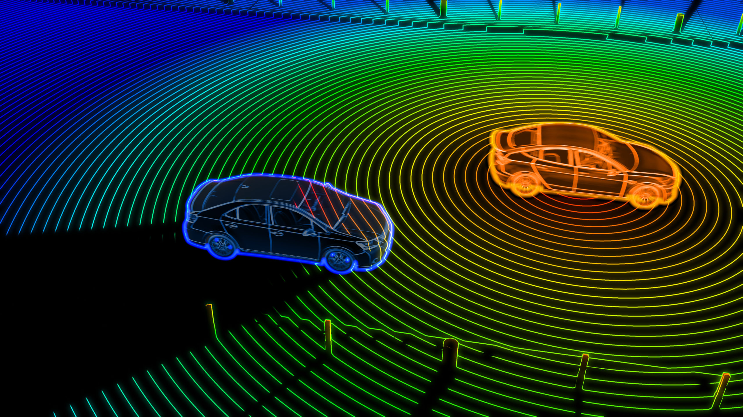
Light Detection and Ranging (LiDAR IP) is a key technology used to detect and map surrounding objects. Along with radar, camera, and ultrasound, it forms the sensor platform for the ongoing development of autonomous vehicles. While radar is robust, reliable, and unaffected by weather conditions, it, in general, lacks the accuracy and resolution that is needed to correctly identify many object types.
Cameras present a visual representation of surroundings, but require significant computing power and lighting and weather conditions can severely impact vision. Ultrasonic sensors are mainly used to detect objects at close range. LiDAR provides both excellent range and high resolution and can be combined with data from other sensors to accurately represent a vehicle’s complete environment. LiDAR technology is less sensitive to field lighting conditions than camera sensing because it actively illuminates targets at infrared wavelengths. It is also not as affected by weather conditions as camera-based sensing. It also provides the longest detection range and higher resolution compared to ultrasound, radar, and camera-based sensing.
Innovations in both hardware and software are expected to accelerate the adoption of LiDAR technology in the automotive industry. This whitepaper offers an overview of LiDAR systems, addresses market requirements, and presents innovative semiconductor intellectual property (IP) components for developing LiDAR products.
Principles of LIDAR Systems
LiDAR relies on the time delay between an emitted and reflected light pulse. In its simplest implementation (Figure 1), a pulse of laser light is emitted and the resulting reflection from the scanned object is detected [1].
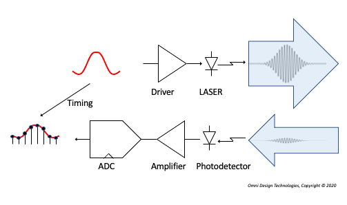
The distance to the detected object can be easily computed because it is represented by half the round-trip time delay
R = c/2 ToF
where R is the distance to the target, c is the speed of light (300,000 km/s in vacuum), and the time of flight (ToF) is the total time elapsed between the emission and detection events. For example, for ToF of 10ns, the measured distance is 1.5m. This process is repeated to scan the surroundings, and the raw data are processed to create a point cloud. A point cloud is a set of data points representing a 3D shape or object. In the case of LiDAR, it refers to the data points representing the objects from the scanned space.
The larger the detection range, the greater the time needed to produce the map because the laser pulse will have to traverse a longer distance. Because of its simplicity, the pulsed-based LiDAR is the most commonly deployed LiDAR system.
Continuous-wave LiDAR
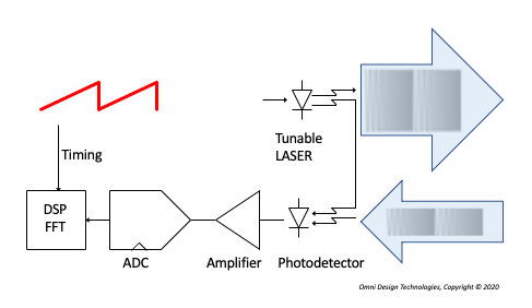
Continuous-wave LiDAR, unlike pulsed LiDAR, uses either amplitude modulation or frequency modulation of the light source. In amplitude-modulated continuous-wave (AMCW) LiDAR, the distance is measured by computing the difference in the phase between the transmitted signal and the received signal [2]. Frequency-modulated continuous-wave (FMCW) LiDAR, (Figure 2) relies on a “chirp,“ a variation of the frequency of the light source over time [2-3].
The transmitted chirp and the returned chirp are mixed at the photodiode, which detects the difference in frequency of those two signals. When the transmitted frequency changes at a constant rate, the difference in frequency between the transmitted and received signal is a direct function of the distance to the target. The beat frequency that results from mixing the two signals represents the distance to the target. Further processing can also extract the target’s relative velocity, and the nature of coherent light makes the system robust against interference.
LiDAR systems typically operate at a wavelength of 905, 1300, or 1550nm [2]. Lasers with a wavelength less than 1400nm can damage the human retina, so the average power must be kept below the level required to comply with eye-safety standards. Lasers with a wavelength of 1550nm are less likely to impact the retina, and thus can support a higher peak-power eye safety level, but they are typically more expensive [4].
LIDAR System Overview
Hardware implementation of a LiDAR system can be accomplished in a few different ways. A common beam-steering implementation is the mechanical spinning LiDAR [2]. Typically mounted on top of the vehicle, the transmitter and receiver assembly physically rotate 360° to scan the environment to achieve a wide field of view (FOV). Although this approach offers detailed mapping with a high signal-to-noise ratio (SNR), the LiDAR module is large and bulky, and the production of such complex mechanical moving parts is expensive. Another concern is low reliability because of mechanical wear and tear of the moving parts in such a module.
MEMS-based LiDAR
A MEMS-based LiDAR implementation is much more affordable and scalable. Because it uses semiconductor manufacturing technology, components can be efficiently mass produced. A MEMS-based LiDAR uses mirrors to electromechanically tilt the light beam to steer it in specific directions. Issues related to robustness in extreme temperature conditions and the impact of large vibrations are still to be addressed. Nonetheless, it is a promising technology for mass deployment [5].
Optical Phased-Array LiDAR
In optical phased-array LiDARs, the beam is steered by waveguides instead of mechanical moving parts [3,6]. This is accomplished by splitting the beam into multiple parts, independently tuning the phase of each, and then using a complex optical antenna array to reradiate the signal. This technique enables shaping and beam steering in the spatial domain. Limited steering angle and side lobes are currently limitations of this technology.
Flash LiDAR operation
Flash LiDAR operation is similar to that of a digital camera. It captures the details of the surroundings in a single flash by illuminating the complete field of view, which leads to mechanical and optical simplicity [7]. It is highly immune to vibration and avoids issues that arise from movements within the LiDAR system during the scan. However, further development is needed to make it suitable for long-range applications.
LIDAR Electronics
Early LiDAR systems for autonomous vehicles were implemented using discrete semiconductor components such as Transimpedance Amplifiers (TIAs), programmable gain amplifiers (PGAs), and analog-to-digital converters (ADCs) assembled on a printed circuit board along with other logic components to demonstrate proof of concept and build low-volume prototypes. In the past few years, developers of autonomous vehicles have adopted the use of LiDAR systems and have started deploying them in production. Autonomous vehicles have begun appearing on public roads with the easily-recognized mechanical spinning LiDAR on the top of the vehicle.
For mass-market adoption of LiDAR solutions, a few different things need to happen. LiDAR components costs have to come down significantly. They must consume an order of magnitude less power than current implementations. Their form factors have to be miniaturized to enable multiple units to be installed behind the automotive skin and they must be more reliable than current solutions.
This has led developers of LiDARs to integrate more of the electronic components, such as TIAs, PGAs, ADCs, and digital logic into a system-on-chip (SoC) to meet the market requirements of performance, power, cost, reliability, and form factor. These SoCs are highly complex and require high performance digital- and mixed-signal circuits to be integrated on the same chip – leading to new design techniques and innovative semiconductor intellectual property (IP) components that enable such SoCs.
SoC LiDAR IP Design Requirements
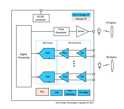
Figure 3 shows a simplified block diagram of a pulse-based LiDAR system [8-10] — the implementation details will vary based on individual system requirements. In the transmitter, a pulse is generated and amplified by the laser driver. The resultant laser beam is then transmitted through the optics. In the receiver, the reflected light signal is detected by the photodiode, which produces a current proportional to the returned signal strength. The current signal is converted to voltage by a transimpedance amplifier (TIA) which was typically implemented as a discrete component outside the SoC. The interface between the photodiode and the TIA is critical as it impacts the LiDAR range precision. A large linear dynamic range is needed in the TIA [8]. A high-speed ADC-based receiver enables sophisticated signal processing of the return signal among other performance advantages [10].
SoC LiDAR IP Quality Requirements
In addition to the previously mentioned specifications, components (including the integrated circuits in the SoC) must meet the requirements set for automotive electronics. AEC-Q100 is an industry standard stress test qualification for integrated circuits. It specifies a temperature grade from 0 to 3 depending on ambient temperature during operation. The components must comply with key test categories that include, but are not limited to, environmental stress, aging, packaging/assembly integrity, electrical verification, die fabrication, among others. In addition to AEC-Q100, there are other AEC-Q standards for discrete semiconductors, optoelectronic devices, passive components, and multi-chip modules.
ISO 26262 is a functional safety standard for electrical and electronic systems in production automobiles. The standard specifies a target Automotive Safety Integrity Level (ASIL) from A (lowest risk level that includes the possibility of equipment damage) to D (highest risk level that includes likelihood of serious injury). SoCs and IPs are typically developed for safety element out of context (SEooC), which allows component developers to define safety performance independently of OEMs and suppliers. Every significant block needs to go through failure modes, effects, and diagnostic analysis (FMEDA) as part of an architecture and design review.
Omni Design’s Solution for LIDAR IP in SoCs
Omni Design offers extremely power-efficient high-performance LiDAR IP cores in advanced process nodes for use in SoCs for LiDARs. These IP cores are compliant with the automotive standards referenced earlier, and cover the full receiver-chain – e.g., front-end TIA, PGA, and data conversion. In addition, Omni Design can integrate many instances of these IP cores to deliver highly complex analog macro blocks that form the core analog/mixed-signal capability of the LiDAR SoC.
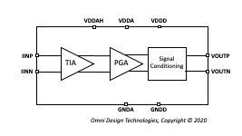
For example, Figure 4 represents an integrated high-performance receiver front-end IP block designed using FinFET technology. The TIA provides current to voltage conversion, which is followed by a PGA, and additional signal conditioning.
Omni Design’s ADC IP cores for use in LiDAR SoCs can deliver sampling rates that range from a few mega samples per second (MSPS) to as high as multi-giga samples per second (GSPS), with resolutions ranging from 10-bits to 14-bits. They are designed to maximize speed while keeping power consumption and silicon area low. They also support other key requirements such as functional safety, synchronized clocking of an ADC array for phased array support, and excellent matching between channels.
For performance-critical LiDAR applications, integration of IPs at the AFE level presents a significant challenge, and careful attention to detail is required. These mega macros must include bumps, ESDs, and may be some third-party phase-locked loop (PLL) IPs. Omni Design has extensive experience designing such analog mega macro blocks that can be integrated into the SoC. We provide all the necessary deliverables to enable the integration of the AFE into the SoC: analog, digital, scan chain, behavioral models, and detailed integration documentation.
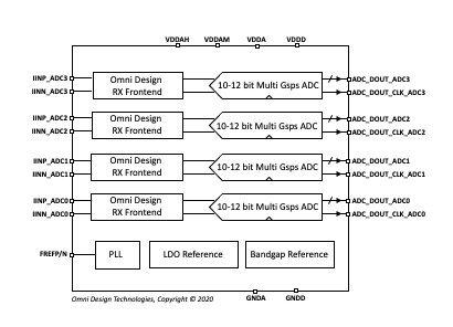
The ODT-AFE-4A1P-12 in Figure 5 is an example of a high-performance AFE IP macro block.
Omni Design’s LIDAR IP Offerings
A partial list of ADC IP cores available from Omni Design is shown in Table 1. These LiDAR IP cores are available in various process nodes, including 28nm and advanced FinFET technologies. The IP cores are designed to include any required foreground and background calibration for correcting various non-idealities, such as time-interleaving artifacts and capacitor mismatch.
| Product Name | Resolution (bits) | Speed (MSPS) |
| ODT-ADP-14B1P2G-28 | 14 | 1200 |
| ODT-ADP-14B600M-28 | 14 | 600 |
| ODT-ADP-14B300M-28 | 14 | 300 |
| ODT-ADP-14B50M-28 | 14 | 50 |
| ODT-ADS-10B2G-28 | 10 | 2000 |
| ODT-ADS-10B150M-28 | 10 | 150 |
| ODT-ADS-6B1G-28 | 6 | 1000 |
| ODT-ADS-6B500M-28 | 6 | 500 |
| ODT-ADS-12B6G-16 | 12 | 6000 |
| ODT-ADS-12B2G-16 | 12 | 2000 |
| ODT-ADS-12B1G-16 | 12 | 1000 |
| ODT-ADS-12B200M-16 | 12 | 200 |
| ODT-ADS-12B20M-16 | 12 | 20 |
| ODT-ADS-10B2P5G-16 | 10 | 2500 |
Table 1. Partial List of ADC IP cores available from Omni Design
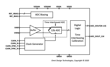
ODT-ADS-12B6G-16, shown in Figure 6, is an example of a high-performance, time-interleaved ADC. This 12-bit 6 Gsps ADC supports input signals up to Nyquist frequency and features SNR and SFDR of 56dB and 62dB, respectively. The design of the data converters leverages Omni Design’s proprietary platform-based development methodology and modular building blocks, resulting in substantial reduction of design schedule risk and an accelerated path to volume production.
Omni Design also offers a broad range of auxiliary IP cores and can integrate them into an analog mega block customized to a customer’s specific requirements. Our process/temperature/voltage (PVT) sensor IP cores offer excellent trimmed and untrimmed temperature and voltage accuracy. We also offer low-dropout voltage regulators (LDOs) that can be used to provide clean supply voltages to analog/mixed-signal IPs. Our bandgap voltage references provide precise, low-noise voltage/current generation for the analog front end.
Summary
As shown in this LiDAR IP whitepaper cost, power consumption, form factor and reliability are critical in enabling mass deployment. These elements are driving a market shift toward use of SoCs that integrate electronic functionality onto a single chip. The SoCs used in LiDAR applications must meet exacting architectural and technology specifications that are continuing to evolve. In addition, automotive reliability and functional safety requirements need to be integrated into the SoC and related component development process. Omni Design offers a broad range of analog mixed-signal IP cores optimized for LiDAR systems. Our development methodology and modular building blocks allow us to integrate these IP cores into mega blocks customized for a customer’s specific requirement.
References
- Royo, S.; Ballesta-Garcia, M. An Overview of Lidar Imaging Systems for Autonomous Vehicles. Appl. Sci. 2019, 9, 4093.
- B. Behroozpour, P. A. M. Sandborn, M. C. Wu and B. E. Boser, “Lidar System Architectures and Circuits,” in IEEE Communications Magazine, vol. 55, no. 10, pp. 135-142, Oct. 2017.
- Christopher V. Poulton, Ami Yaacobi, David B. Cole, Matthew J. Byrd, Manan Raval, Diedrik Vermeulen, and Michael R. Watts, “Coherent solid-state LIDAR with silicon photonic optical phased arrays,” Opt. Lett. 42, 4091-4094 (2017)
- R. Thakur, “Scanning LIDAR in Advanced Driver Assistance Systems and Beyond: Building a road map for next-generation LIDAR technology,” in IEEE Consumer Electronics Magazine, vol. 5, no. 3, pp. 48-54, July 2016.
- Yoo, H.W., Druml, N., Brunner, D. et al. MEMS-based lidar for autonomous driving. Elektrotech. Inftech. 135, 408–415 (2018)
- C. V. Poulton et al., “Long-Range LiDAR and Free-Space Data Communication With High-Performance Optical Phased Arrays,” in IEEE Journal of Selected Topics in Quantum Electronics, vol. 25, no. 5, pp. 1-8, Sept.-Oct. 2019, Art no. 7700108.
- M. E. Warren, “Automotive LIDAR Technology,” 2019 Symposium on VLSI Circuits, Kyoto, Japan, 2019, pp. C254-C255.
- R. Ma, M. Liu, H. Zheng and Z. Zhu, “A 66-dB Linear Dynamic Range, 100-dB· W Transimpedance Gain TIA With High-Speed PDSH for LiDAR,” in IEEE Transactions on Instrumentation and Measurement, vol. 69, no. 4, pp. 1020-1028, April 2020.
- H. Zheng, R. Ma, M. Liu and Z. Zhu, “A Linear-Array Receiver Analog Front-End Circuit for Rotating Scanner LiDAR Application,” in IEEE Sensors Journal, vol. 19, no. 13, pp. 5053-5061, 1 July1, 2019.
- K. Yoshioka et al., “A 20-ch TDC/ADC Hybrid Architecture LiDAR SoC for 240 X 96 Pixel 200-m Range Imaging With Smart Accumulation Technique and Residue Quantizing SAR ADC,” in IEEE Journal of Solid-State Circuits, vol. 53, no. 11, pp. 3026-3038, Nov. 2018.